Index
- Specifications
- Fetch
- Instruction Memory
- Decode
- Register File
- Execute
- ALU
- Load Store
- Hazard
- CPU
- Verification
- Sample Assembly Program
Specifications
- Pipeline Stages - Fetch, Decode, Execute, Load-Store, Writeback
- Handles only integer instructions
- Cycles Per Instruction = 5
- Max. Instructions Per Cycle = 1
- Clock Frequency = 200 MHz (Max. in FPGA without any scaling)
- 4KB Instruction Memory and 4KB Data Memory (12-bit address as given in RISC-V ISA)
- 32 registers (As given in RISC-V ISA)
- Handles Data, Structural, and Control Hazards
- Static Branch Prediction - Assumes the branch is never taken
Fetch
- Fetches one instruction 32-bit from memory every clock cycle.
- Program Counter gets incremented by 4
- If a branch is detected, PC gets updated to the value received as pc_imm
- If a stall is detected, the PC is maintained
RTL:
module ifu(
    input clk_i
    ,input reset_i
    ,input branch_en
    ,input stall
    ,input signed [19:0] pc_imm
    ,output logic [31:0] instruction_o
    ,output logic [31:0] PC
    );

 initial begin
    PC = 32'b0;  // 32-bit program counter is initialized to zero
 end
        programMemory progMem(
        .addr_i(PC)
       ,.data_o(instruction_o)
       );

        always @(posedge clk_i, posedge reset_i)
        begin
            if (reset_i == 1) begin
                PC <= 0;
            end
            else if (stall)
            begin
                PC <= PC;
            end
            else if (branch_en == 1) begin
                PC[19:0] <= PC[19:0] + pc_imm - 4;
            end
            else
            begin
                PC <= PC + 4;
            end
        end
endmodule
Instruction Memory
- Implemented a 4KB Asynchronous ROM
- Vivado can synthesize an initial block if it’s RAM
- Gets synthsized into LUTs since it’s asynchronous
RTL:
module programMemory(
    input [31:0] addr_i,
    output logic [31:0] data_o
    );

    reg [7:0] memory[127:0];

    //Vivado can actually synthesize initial block for RAM
    initial
        begin
            $readmemh("helloworld.mem", memory);		//Hex program is read
        end

    assign data_o = (addr_i < 127) ? {memory[addr_i[6:0]+3],memory[addr_i[6:0]+2],memory[addr_i[6:0]+1],memory[addr_i[6:0]]} : 32'b0;

endmodule
Decode
- Handles bulk of the control. Decodes the instruction and sets some of the following.
- Control bits for the Execute unit (arithmetic or logical and enable)
- Address for the register file (To fetch OP1, OP2 and store Result)
- Control for the memory (address + enables)
- Control for the branch instruction (to detect if the instruction is a branch)
The full module is not captured here since it’s long. You can find the source in my github repo.
Core of the RTL:
always_comb
    begin
        if (reset_i)
        begin
            alu_control = 4'b1111;
            rs1_address = 0;
            rs2_address = 0;
            pcIMM = 0;
            rf_writeAddress = 0;
            memoryAddress = 0;
            rf_writeEnable = 0;
            outputEnable = 0;
            immediate = 0;
        end
        else if (opcode == 7'b0110011)
        begin
            case(funct3)
            0: begin
                if(funct7==0)
                alu_control= 4'b0000; //ADD
                else
                alu_control= 4'b1000; //SUB
            end
            1: alu_control= 4'b0001; //SLL
            2: alu_control= 4'b0010; //SLT
            3: alu_control= 4'b0011;//SLTU
            4: alu_control= 4'b0100; // XOR
            5: begin
                if(funct7==0)
                alu_control= 4'b0101; //SRL
                else
                alu_control= 4'b1001; //SRA
            end
            6: alu_control= 4'b0110; // OR
            7: alu_control= 4'b0111; // AND
            default: alu_control = 4'b1111;
            endcase
            rs1_address = instruction_i[19:15];
            rs2_address = instruction_i[24:20];
            immediate = 0;
            pcIMM = 0;
            rf_writeAddress = instruction_i [11:7];
            memoryAddress = 0;
            rf_writeEnable = 1;
            outputEnable = 0;
        end
Register File
- 32 Registers of 32-bits as specified by the ISA
- 2R1W ports
To avoid contention and resolve data dependencies:
- Read happens in the positive edge of the clock
- Write happens in the negative edge of the clock
RTL:
module registerFile(
      input write_enable
    , input clk_i
    , input reset_i
    , input [4:0] rs1_address
    , input [4:0] rs2_address
    , input [4:0] write_address
    , input [31:0] write_data
    , output logic [31:0] rs1
    , output logic [31:0] rs2
    );

    reg [31:0] x[0:31];
    integer i;

    always @(posedge clk_i, posedge reset_i)
    begin
        if (reset_i)
          begin
            for(i=0;i<=31;i=i+1)
                begin x[i] <= 32'b0; end
          end
        else if (write_enable)
                begin
                x[write_address] <= write_data;
                x[0] <= 0;
                end
        else
        begin
            x[0] <= 0;
        end
    end

    always @(negedge clk_i, posedge reset_i)
    begin
        if (reset_i)
          begin
            rs1 <= 0;
            rs2 <= 0;
          end
        else begin
                rs1 <= x[rs1_address];
                rs2 <= x[rs2_address];
                end
    end
endmodule
Execute
- Receives control instructions from the decode stage and forwards it appropriately
- Acts like a wrapper for the ALU
- If ALU is not enabled, it forwards the input to memory.
module execute(
    input clk_i
  , input reset_i
  , input signed [31:0] r1
  , input signed [31:0] r2
  , input [3:0] alu_control
  , input mem_en_i
  , input mem_wr_i
  , input [10:0] mem_addr_i
  , input [4:0] wbAddr_i
  , input wbEnable_i
  , input displayEn_i
  , input stall
  , output logic [31:0] data_o
  , output logic mem_en_o
  , output logic mem_wr_o
  , output logic [10:0] mem_addr_o
  , output logic [4:0] wbAddr_o
  , output logic wbEnable_o
  , output logic displayEn_o
  );

  logic [31:0] alu_result;

  alu ALU_module(
      .r1(r1),
      .r2(r2),
      .alu_control(alu_control),
      .alu_result(alu_result)
      );

  always @ (posedge clk_i, posedge reset_i)
  if (reset_i == 1 | stall == 1) begin
    mem_en_o <= 0;
    mem_wr_o <= 0;
    mem_addr_o <= 0;
    wbAddr_o <= 0;
    wbEnable_o <= 0;
    displayEn_o <= 0;
    data_o <= 0;
  end
  else
  begin
      wbAddr_o <= wbAddr_i;
      wbEnable_o <= wbEnable_i;
      data_o <= alu_result;
      mem_en_o <= mem_en_i;
      mem_wr_o <= mem_wr_i;
      mem_addr_o <= (mem_en_i == 1) ? alu_result : 0;
      displayEn_o <= displayEn_i;
  end
endmodule
ALU
Does arithmetic and logic instructions
module alu (
  input signed [31:0] r1
, input signed [31:0] r2
, input [3:0] alu_control
, output logic signed [31:0] alu_result
);

always_comb
    begin
        case(alu_control)
            4'b0000: alu_result = r1 + r2;
            4'b0001: alu_result = r1<<r2[4:0]; //shift left logical SLL
            4'b0010: begin
            if(r1<r2)
                alu_result = 1;
            else
                alu_result = 0;
                end
            4'b0011: begin
                if($unsigned(r1) < $unsigned(r2))
                    alu_result = 1;
                else
                    alu_result = 0;
                end
            4'b0100: alu_result = r1^r2;
            4'b0101: alu_result = r1 >> r2[4:0]; //shift right logical SRL
            4'b0110: alu_result = r1 | r2;
            4'b0111: alu_result = r1 & r2;
            4'b1000: alu_result = r1 - r2;
            4'b1001: alu_result = $signed(r1) >>> r2[4:0]; //shift right arithmetic SRA //Need to check this
            4'b1010: alu_result = r1 << r2; //shift left logical immediate SLLI
            4'b1011: alu_result = r1 >> r2; //shift right logical immediate SRLI
            4'b1100: alu_result = $signed(r1) >>> r2; //shift right arithmetic immediate SRAI //Need to check this
            4'b1101: alu_result = r1 << 12; //LUI
            default: alu_result = 0;

        endcase
    end
endmodule
Load Store
- 4KB Synchronous 1RW SRAM
- Inferred Block RAM
- If memory is not enabled, it forwards the result to writeback
RTL:
module dataMemory(
    input clk_i,
    input reset_i,
    input mem_en,
    input [10:0] addr_i,
    input wr_en,
    input [31:0] data_i,
    input [4:0] wbAddr_i,
    input wbEnable_i,
    output logic [31:0] data_o,
    output logic [4:0] wbAddr_o,
    output logic wbEnable_o
    );

    reg [7:0] ram [63:0];

    always @ (posedge clk_i, posedge reset_i)
    begin
        if (reset_i == 1) begin
            $readmemh("data.mem", ram);
            wbAddr_o <= 0;
            wbEnable_o <= 0;
            data_o <= 0;
        end
        else if (wr_en & mem_en)
        begin
            wbAddr_o <= wbAddr_i;
            wbEnable_o <= wbEnable_i;
            data_o <= 0;
            {ram[addr_i[5:0]+3],ram[addr_i[5:0]+2],ram[addr_i[5:0]+1],ram[addr_i[5:0]]} <= data_i;
        end
        else if (mem_en)
        begin
            wbAddr_o <= wbAddr_i;
            wbEnable_o <= wbEnable_i;
            data_o <= {ram[addr_i[5:0]+3],ram[addr_i[5:0]+2],ram[addr_i[5:0]+1],ram[addr_i[5:0]]};
        end
        else
        begin
            data_o <= data_i;
            wbAddr_o <= wbAddr_i;
            wbEnable_o <= wbEnable_i;
        end
    end
endmodule
Hazard Unit
- Detects Data or Control Hazards
- In case of Data Hazards, the appropriate Muxes are controlled to enable forwarding
- In case of Control Hazards, the pipeline is stalled or flushed
- Pipeline is stalled during Read-after-Write Hazard in Register File
- Pipeline is flushed if a branch is taken
RTL:
module hazardUnit(
    input clk_i,
    input reset_i,
    input [4:0] rs1,
    input [4:0] rs2,
    input [4:0] alurd_i,
    input [4:0] loadrd_i,
    input memEn_i,
    input memWr_i,
    input signed [31:0] op1_i,
    input signed [31:0] op2_i,
    input signed [31:0] aluResult,
    input signed [31:0] loadResult,
    output logic signed [31:0] op1_o,
    output logic signed [31:0] op2_o,
    output logic stall
    );

    logic [4:0] rs1_i, rs2_i;
    logic stall_n;

    always_comb
    begin
        if (reset_i)
        begin
            stall_n = 0;
            op1_o = 0;
            op2_o = 0;
        end
        else if (stall == 1)
            begin
                if((rs1_i == loadrd_i) & (rs1_i != 0))
                        begin
                            stall_n = 0;
                            op1_o = loadResult;
                            op2_o = op2_i;
                        end
                        else if ((rs2_i == loadrd_i) & (rs2_i != 0))
                        begin
                            stall_n = 0;
                            op1_o = op1_i;
                            op2_o = loadResult;
                        end
                        else if ((rs1_i == loadrd_i) & (rs2_i == loadrd_i) & (rs1_i != 0) & (rs2_i != 0))
                        begin
                            stall_n = 0;
                            op1_o = loadResult;
                            op2_o = loadResult;
                        end
                        else
                        begin
                            stall_n = 0;
                            op1_o = op1_i;
                            op2_o = op2_i;
                        end
            end
        else if ((memEn_i == 0) & (memWr_i == 0))
        begin
            stall_n = 0;
            if((rs1_i == alurd_i) & (rs1_i != 0))
            begin
                op1_o = aluResult;
                op2_o = op2_i;
            end
            else if ((rs2_i == alurd_i) & (rs2_i != 0))
            begin
                op1_o = op1_i;
                op2_o = aluResult;
            end
            else if ((rs1_i == alurd_i) & (rs2_i == alurd_i) & (rs1_i != 0) & (rs2_i != 0))
            begin
                op1_o = aluResult;
                op2_o = aluResult;
            end
            else
            begin
            op1_o = op1_i;
            op2_o = op2_i;
            end
        end
        else if ((memEn_i == 1) & (memWr_i == 0))
        begin
            if((rs1_i == alurd_i) & (rs1_i != 0))
            begin
                stall_n = 1;
                op1_o = 0;
                op2_o = 0;
            end
            else if ((rs2_i == alurd_i) & (rs2_i != 0))
            begin
                stall_n = 1;
                op1_o = 0;
                op2_o = 0;
            end
            else if ((rs1_i == alurd_i) & (rs2_i == alurd_i) & (rs1_i != 0) & (rs2_i != 0))
            begin
                stall_n = 1;
                op1_o = 0;
                op2_o = 0;
            end
            else
            begin
                stall_n = 0;
                op1_o = op1_i;
                op2_o = op2_i;
            end
        end
        else
        begin
            stall_n = 0;
            op1_o = op1_i;
            op2_o = op2_i;
        end
    end

    always @(posedge clk_i, posedge reset_i)
    begin
        if(reset_i)
        begin
            rs1_i <= 0;
            rs2_i <= 0;
            stall <= 0;
        end
        else
        begin
            stall <= stall_n;
            rs1_i <= rs1;
            rs2_i <= rs2;
        end
    end
endmodule
Top Level
All the modules are wired together
RTL:
module cpu(
     input clk_i,
     input reset_i,
     output logic [6:0] led
    );

    logic [31:0] instruction, pc;               //IFU to CU
    logic [19:0] pc_imm;                    //CU to IFU
    logic branchEnable;                     //CU to IFU
    logic [31:0] op1, op2, operand1, operand2;                  //CU to Execute
    logic [3:0] aluControl;                 //CU to Execute
    logic [31:0] executeData;               //Execute to Data Memory
    logic memoryEnable1, memoryWrite1, memoryEnable2, memoryWrite2;  //CU to Execute to Data Memory
    logic [10:0] memoryAddress1, memoryAddress2;             //CU to Execute to Data Memory
    logic [31:0] registerData;              //Data Memory to CU Register
    logic [4:0] writeBackAddress1, writeBackAddress2, writeBackAddress3;           //CU to Execute to Memory to CU
    logic writeBackEnable1, writeBackEnable2, writeBackEnable3;                   //CU to Execute to Memory to CU
    logic displayEn1, displayEn;                        //CU to Display
    logic [4:0] rs1Addr, rs2Addr;
    logic stall;

    ifu fetch (
     .clk_i(clk_i)
    ,.reset_i(reset_i)
    ,.stall(stall)
    ,.instruction_o(instruction)
    ,.branch_en(branchEnable)
    ,.pc_imm(pc_imm)
    ,.PC(pc)
    );

    controlUnit decode (
     .clk_i(clk_i)
    ,.reset_i(reset_i)
    ,.instruction_i(instruction)
    ,.write_data(registerData)
    ,.aluControl_o(aluControl)
    ,.op1(op1)
    ,.op2(op2)
    ,.mem_en(memoryEnable1)
    ,.mem_wr(memoryWrite1)
    ,.mem_addr(memoryAddress1)
    ,.pc_i(pc)
    ,.branch_en(branchEnable)
    ,.pc_imm(pc_imm)
    ,.displayEn_o(displayEn1)
    ,.wbAddr_i(writeBackAddress3)
    ,.wbEnable_i(writeBackEnable3)
    ,.wbAddr_o(writeBackAddress1)
    ,.wbEnable_o(writeBackEnable1)
    ,.rs1_address(rs1Addr)
    ,.rs2_address(rs2Addr)
    ,.stall(stall)
    );

    hazardUnit hazard (
     .rs1(rs1Addr)
    ,.rs2(rs2Addr)
    ,.clk_i(clk_i)
    ,.reset_i(reset_i)
    ,.alurd_i(writeBackAddress2)
    ,.loadrd_i(writeBackAddress3)
    ,.aluResult(executeData)
    ,.loadResult(registerData)
    ,.op1_i(op1)
    ,.op2_i(op2)
    ,.op1_o(operand1)
    ,.op2_o(operand2)
    ,.memEn_i(memoryEnable2)
    ,.memWr_i(memoryWrite2)
    ,.stall(stall)
    );

    execute execute (
     .clk_i(clk_i)
    ,.reset_i(reset_i)
    ,.alu_control(aluControl)
    ,.r1(operand1)
    ,.r2(operand2)
    ,.mem_en_i(memoryEnable1)
    ,.mem_wr_i(memoryWrite1)
    ,.mem_addr_i(memoryAddress1)
    ,.mem_en_o(memoryEnable2)
    ,.mem_wr_o(memoryWrite2)
    ,.mem_addr_o(memoryAddress2)
    ,.displayEn_i(displayEn1)
    ,.displayEn_o(displayEn)
    ,.data_o(executeData)
    ,.wbAddr_i(writeBackAddress1)
    ,.wbEnable_i(writeBackEnable1)
    ,.wbAddr_o(writeBackAddress2)
    ,.wbEnable_o(writeBackEnable2)
    ,.stall(stall)
    );

    dataMemory memory (
     .clk_i(clk_i)
    ,.reset_i(reset_i)
    ,.mem_en(memoryEnable2)
    ,.addr_i(memoryAddress2)
    ,.wr_en(memoryWrite2)
    ,.data_i(executeData)
    ,.data_o(registerData)
    ,.wbAddr_i(writeBackAddress2)
    ,.wbEnable_i(writeBackEnable2)
    ,.wbAddr_o(writeBackAddress3)
    ,.wbEnable_o(writeBackEnable3)
    );

    display hexa (
     .clk_i(clk_i)
    ,.reset_i(reset_i)
    ,.hex_i(executeData[7:0])
    ,.displayEn_i(displayEn)
    ,.display_o(led)
    );

endmodule
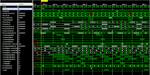
Verification
- Wrote directed testbenches for each module in the processor
- All testbenches can be found in the repo
- Wrote different assembly programs to verify the working of the entire processor
- Analyzed waveforms using the Vivado waveform viewer
Sample Assembly Program
# arr = {6, 1, 3, 2, 7}
LI a0, 0x10000000 # start address
LI a1, 0x10000000 # Reference start address
LI a2, 6
SB a2,0(a0)
LI a2, 1
SB a2,4(a0)
LI a2, 3
SB a2,8(a0)
LI a2, 2
SB a2,12(a0)
LI a2, 7
SB a2,16(a0)

# Register Map:
# a0 - Start Address
# a1 - Address Reference
# a2 - Load values
# a3 - Store the size of input array
# a4 - Used for incrementing the first loop
# a5 - Used to define size of second loop
# a6 - Used for incrementing second loop
# a7 - stores size of each element
# t0 - Operator for first loop
# t1 - Operator for second loop
# t2 - Stores binary value of swapped variable
# t3 - Used to load and swap
# t4 - Used to load and swap

# .global bubbleSort

bubbleSort:
LI a3, 5    # Stores size of array
LI a4, 1    # Used for incrementing the loop
LI a5, 4    # Used as size of array - 1 for subloop
LI a7, 4    # Memory Address Increment Size

loop1:
LI t2, 0   # Setting swapped = false

loop2:
LB t3, 0(a1) #Address
LB t4, 4(a1)#Address + 4
BLT t4,t3,swap

J continue

swap:
SB t4, 0(a1)#Address
SB t3, 4(a1)#Address + 4
LI t2,1  # Setting swapped = true

continue:
ADD a1,a1,a7 # Increment Memory Address
ADD t1,t1,a4 # Increment t1 by 1
SUB a6,a5,t0 # a6 = loop - i - 1
BLT t1,a6,loop2 # Check if t1 = loop - i - 1
LI t1, 0      #Set t1 = 0 to initialize loop2
ADD t0,t0,a4  # Increment t0 by 1
BEQ t2,t1,test #replace end with test to retrieve data from memory and store from a1-a5

LI a1, 0x10000000 # Setting a1 back to old memory
BLT t0,a3,loop1 #Check if t0 = size of array

test:
LB a1, 0(a0)
LB a2, 4(a0)
LB a3, 8(a0)
LB a4, 12(a0)
LB a5, 16(a0)